SPD

I had an old SDR SDRAM DIMM module which showed errors around a particular address. I tried forcing the computer to avoid the problematic area by modifying the SPD (Serial Presence Detect) EEPROM.

Contents

Structure of a module

Chips usually store data in three dimensions: rows (X), columns (Y), and banks (Z). Address pins are shared between the row and the column, and switched by CAS and RAS signals. Given a row, column and bank, 8 chips, no ECC and 8 bits of output per chip we get a native data width of 64 bits, or 8 bytes.

The mapping from "physical" (as compared to virtual) memory to address inputs is typically this, going from the most to the least significant bit: row, bank, column. Memory controllers may decide to make this relationship slightly more complex, e.g. by XORing some bits together.

Reprogramming

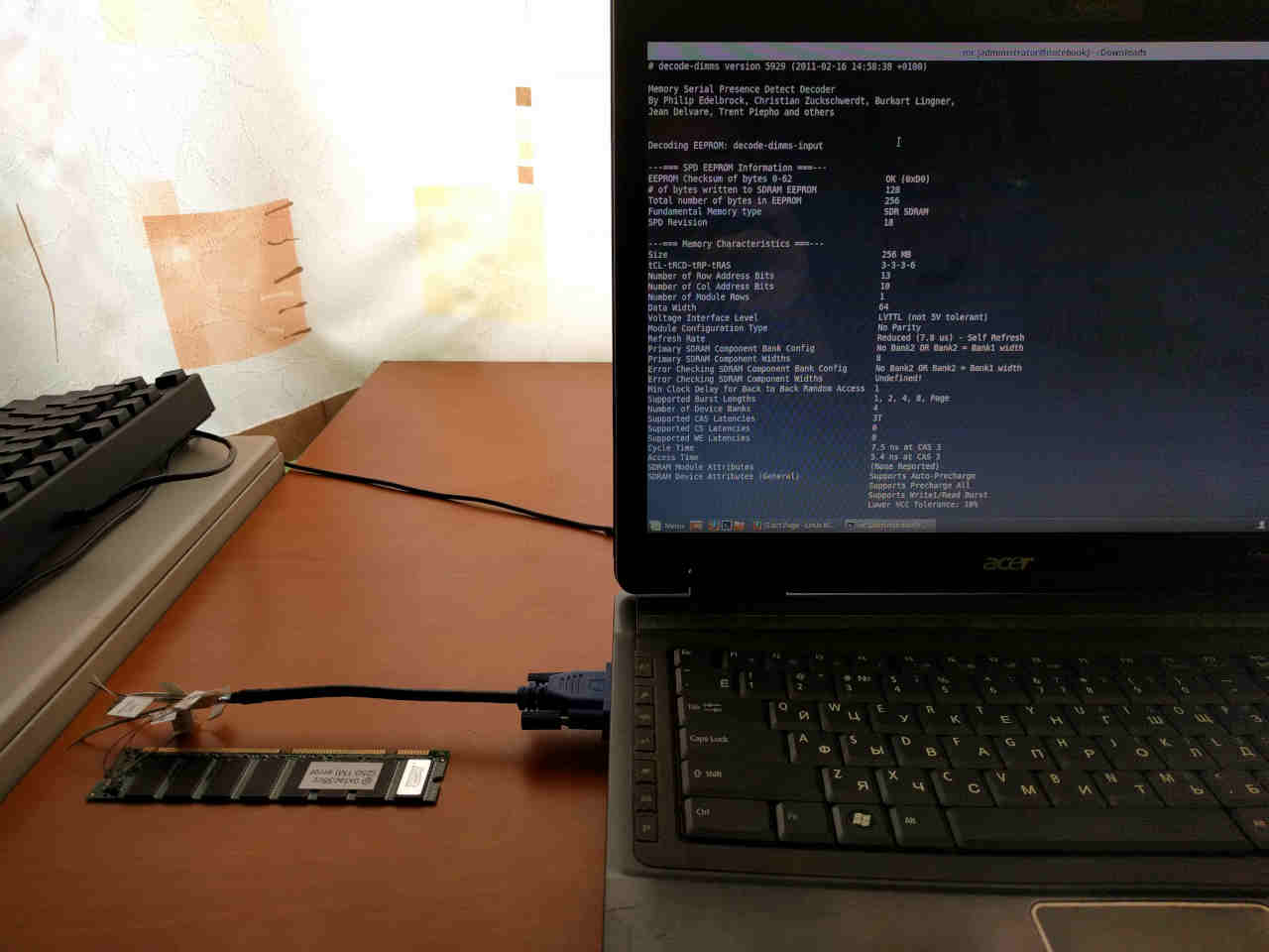
To reprogram the SPD I used a spare VGA cable and an old laptop, making use of the I2C interface used to read out display information: Cut the cable near the connector, split the subcables and label them with help of a multimeter and pinout information. Then solder +5V, GND, SCL and SDA directly to the SPD chip according to the pinout in its datasheet (search by part number). Connect address pins to ground so that the chip is at the address of 0x50 (incidentally the same as the EDID chip of a monitor). If you can’t find a datasheet, follow traces to the respective nearby DIMM pins. The EEPROM should be 5V-tolerant, or another means is required.

I ran modprobe i2c-dev to make the I2C interface show up as /dev/i2c-$number, connected a monitor and used my DDC/CI tool to figure out which device number it would succeed with.

Then I plugged in the modified VGA cable and used i2c-tools to read out and modify SPD contents. xxd is a useful tool for making an input file for decode-dimms, although the output requires some touch-ups.

1280

DVI, HDMI and DisplayPort can also be used for easy access to an I2C bus, there’s just more wires to worry about.

Results

I have tried reducing the reported number of banks, rows, and columns, effectively "halving" the memory module in different dimensions. I have always fixed up the row density (byte 31) and the checksum (byte 63) accordingly. See the SPD specification for details.

Both computers I tried the modified memory module in ignored my changes and kept reporting the same module size as shown by the BIOS during boot. I even tried cutting the A13 and A12 traces in hope that the module size is determined electrically but that did nothing.

Failure.

Possible further research: BIOS disassembly and reverse engineering. Figure out how it detects the memory module size—​the BIOS should progressively go through the following stages during boot: no memory at all, L1/L2 cache configured as memory, memory fully configured.

Comments

Use e-mail, webchat, or the form below. I'll also pick up on new HN, Lobsters, and Reddit posts.